Your circuit works perfectly in isolation. You connect it to the rest of the system and things start going wrong. A nearby motor drive causes data corruption on a serial bus. An oscilloscope readout shows noise spikes that were not there during benchtop testing. The wireless module drops packets when the power supply switches. These are classic symptoms of electromagnetic interference, and they cost engineering teams significant time during integration, certification, and production.
Understanding what EMI radiation is, where it comes from, how it couples into other circuits, and how EMC testing identifies and quantifies it gives you the framework to design products that work reliably in the real world - and that pass regulatory certification without expensive re-spins.
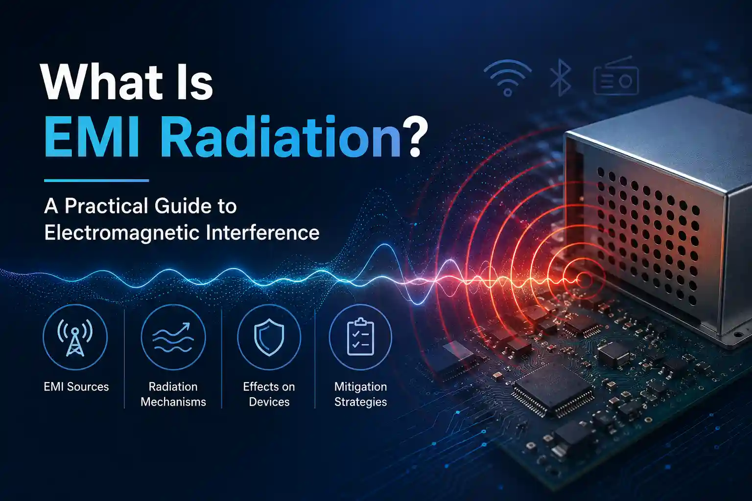
EMI Full Form and Definition
EMI stands for Electromagnetic Interference. It refers to electromagnetic energy emitted by one device or conductor that degrades the performance of another device in its vicinity. The IEC standard IEC 61000 defines EMI as 'electromagnetic disturbance that may degrade the performance of a device, equipment, or system.'
EMI is sometimes called radio frequency interference (RFI), particularly when the interfering energy falls in the radio frequency portion of the spectrum (above roughly 10 kHz). The two terms are often used interchangeably in practice, though EMI is the broader and more technically precise designation.
EMI is a physical reality in any system where current changes over time. Every switching event - in a power supply, a microcontroller, a motor drive, or even a digital signal line - radiates energy. The question is not whether your design emits electromagnetic energy, but whether that emission is controlled and contained to levels that do not affect other equipment.
What Causes EMI Radiation?
EMI originates from any source of rapidly changing current or voltage. Understanding the root causes helps identify which parts of a design are likely to be the primary emitters.
Natural Sources
Lightning discharges generate broadband electromagnetic pulses that can induce transients on power lines and data cables. Solar activity, particularly geomagnetic storms, can induce currents in long conductors. Electrostatic discharge (ESD) from human contact is another natural source that is particularly destructive to unprotected semiconductor inputs.
Switching Power Supplies
SMPS circuits are among the most significant man-made EMI sources in electronic equipment. The high-frequency switching transistor produces a fast-rising current waveform with energy content extending well above the fundamental switching frequency. An SMPS switching at 100 kHz generates harmonics at 200 kHz, 300 kHz, and further up through the megahertz range. Layout, shielding, and input filtering are the primary tools for controlling SMPS emissions.
Digital Clocks and Data Lines
Every digital signal transition is a source of radiated EMI. A microprocessor running at 100 MHz and its associated DDR memory interface, PCIe bus, and USB connections collectively represent dozens of high-frequency sources on a single board. The rise and fall times of digital signals (not their frequency alone) determine how much high-frequency energy they radiate.
Motors and Variable-Speed Drives
Electric motors, particularly brushed DC and BLDC designs driven by PWM inverters, are powerful broadband EMI sources. The commutation switching and associated parasitic capacitances couple interference onto motor cables, which then act as antennas radiating emissions across a wide frequency range.
RF Transmitters and Wireless Modules
Wi-Fi, Bluetooth, Zigbee, and cellular modules are by design sources of narrowband RF emissions centred on their operating frequency. Their emissions are licensed and limited by regulatory standards, but they can still interfere with other circuits operating in or near the same frequency band.
Types of EMI
EMI is classified by how it propagates from its source to the affected device. The two primary categories drive different testing methodologies and different mitigation strategies.
Radiated EMI
Radiated EMI propagates through the air as electromagnetic waves, without any physical conductor connecting the source and the victim. Cables, PCB traces, and enclosure openings act as antennas that either radiate energy outward or receive energy from external sources. Radiated emission limits are enforced from 30 MHz to 1 GHz (and in some standards, up to 6 GHz) by FCC Part 15, CISPR 32, and similar regulations.
Conducted EMI
Conducted EMI travels along conductors - power cables, ground planes, signal lines - connecting different parts of a system. A switching power supply's input filter, for example, is specifically designed to prevent high-frequency switching noise from travelling back up the mains cable and affecting other equipment on the same power circuit. Conducted emission standards apply from 150 kHz to 30 MHz.
EMI vs EMC - What Is the Difference?
The two terms are closely related but describe different aspects of the same problem.
EMI (Electromagnetic Interference) describes the emission or the disturbance itself - the electromagnetic energy that is causing or could cause a problem.
EMC (Electromagnetic Compatibility) describes a device's ability to function as intended in its electromagnetic environment without causing unacceptable interference to other devices. A device is said to be EMC-compliant when it meets two criteria: its emissions are below the regulatory limits, and it is sufficiently immune to interference from other sources.
In other words, EMI is the problem, and EMC is the discipline and set of standards that define how to measure, limit, and manage that problem.
| Aspect | EMI | EMC |
| Definition | The electromagnetic disturbance itself | Ability to operate without causing or suffering interference |
| Scope | Specific emission or susceptibility event | Overall system-level discipline and compliance |
| Regulatory focus | Emission limits (FCC, CISPR) | Both emissions and immunity (IEC 61000 series) |
| Design goal | Minimise emissions | Meet both emission limits and immunity thresholds |
Why EMI Matters for Product Design
EMI compliance is not optional for most electronic products. Regulatory bodies in every major market require that products meet defined emission and immunity limits before they can be sold.
Regulatory Requirements
In India, BIS certification under the Electronics and Information Technology Goods (Requirements for Compulsory Registration) Order mandates EMC compliance for a wide range of consumer and industrial electronics. Exports to the US require FCC Part 15 compliance; exports to Europe require the CE mark, which includes EMC compliance under the EU EMC Directive 2014/30/EU. Products that fail regulatory testing cannot legally be sold in those markets.
System-Level Reliability
Beyond regulatory compliance, EMI affects the functional reliability of systems in the field. Industrial equipment operating near motor drives, automotive electronics exposed to ignition noise, and medical devices sharing a power circuit with other hospital equipment all face real-world EMI challenges. Designing for adequate immunity margins reduces field failures and warranty costs.
How EMI/EMC Testing Works
EMC testing quantifies a device's emissions and immunity against defined limits. Testing is conducted in specialised facilities that control the electromagnetic environment to ensure repeatable measurements.
Emission Testing
Radiated emission testing is performed in a semi-anechoic chamber (SAC) or open-area test site (OATS), where the device under test operates at its worst-case configuration while calibrated antennas measure the electromagnetic field strength at a specified distance (typically 3m or 10m). Conducted emission testing is performed using a line impedance stabilisation network (LISN), which presents a standardised impedance to the device's power input while a spectrum analyser measures the conducted noise.
Immunity Testing
Immunity tests expose the device to defined interference levels and verify that it continues to function within specification. Common immunity tests include radiated immunity (CISPR 24 / IEC 61000-4-3), ESD immunity (IEC 61000-4-2), electrical fast transient (EFT) immunity (IEC 61000-4-4), and surge immunity (IEC 61000-4-5). Each test applies a specific interference type, level, and duration.
Pre-Compliance Testing vs Full Compliance Testing
Full compliance testing is conducted at an accredited third-party lab using calibrated chambers and equipment that directly generate the certification data. Pre-compliance testing is conducted earlier in the development process, typically in a non-accredited lab using near-field probes, a spectrum analyzer for EMI pre-compliance, and a current probe on the power cable. Pre-compliance testing does not produce certification data, but it identifies problem areas in the design before the cost of formal certification testing is incurred.
Engineering teams that run pre-compliance testing before formal lab submission consistently report fewer failed submissions and shorter overall certification timelines. Identifying a radiated emission peak above the CISPR 32 Class B limit in your own lab during development is far less expensive than discovering it at the accredited test facility with a product launch deadline approaching. Advanced instruments such as Anritsu signal spectrum analyzers can help engineers detect and troubleshoot emission issues early, improving the likelihood of passing formal compliance testing on the first attempt.
Common EMI Mitigation Techniques
Most EMI problems encountered during development and testing respond to a well-understood set of mitigation techniques. The choice of technique depends on whether the problem is radiated or conducted, and whether the product is over its emission limit or failing an immunity test.
Shielding
A conductive enclosure reflects and absorbs electromagnetic energy, reducing both radiated emissions escaping from the product and external interference entering it. The effectiveness of shielding depends on the conductivity of the material, the thickness, and critically, the integrity of seams, apertures, and cable penetrations. A single unsealed opening or unfiltered cable can defeat an otherwise effective shield.
Filtering
EMI filters on power lines and signal cables attenuate high-frequency conducted noise. A typical mains EMI filter combines common-mode chokes and X/Y capacitors to suppress both common-mode and differential-mode conducted noise. On signal lines, ferrite beads and RC networks attenuate high-frequency components while preserving the intended signal bandwidth.
PCB Layout
The majority of EMC problems can be prevented at the PCB layout stage before any filtering or shielding is added. Key layout practices include keeping switching current loops as small as possible, using a solid ground plane, placing decoupling capacitors close to IC power pins, routing high-speed signal traces away from I/O connectors, and using differential signalling for long traces.
Grounding
Poor grounding is the root cause of a large proportion of EMC failures. A ground plane that is split, interrupted, or shared between noisy and sensitive circuits allows noise currents to generate voltage differences that drive both emissions and susceptibility. Single-point grounding for sensitive analog circuits and low-impedance ground planes for digital and power circuits are established best practices.
Pre-Compliance EMI Testing in India
Access to pre-compliance EMI testing has historically been a challenge for Indian electronics manufacturers, given the limited availability of accredited EMC test facilities outside of the major metro areas and the cost of sending prototypes overseas for early-stage evaluation.
Revinetech operates a pre-compliance EMI/EMC lab in Pune that is equipped to perform radiated and conducted emission scans, near-field EMI mapping, and basic immunity testing on prototype hardware. Engineering teams can use the pre-compliance EMI/EMC testing service at Revinetech to identify emission peaks, evaluate the effectiveness of mitigation techniques, and build confidence before formal certification submission.
In addition to EMI measurements, engineers often rely on an oscilloscope for signal and noise debugging to investigate switching noise, transient events, and other signal integrity issues that can contribute to EMC failures.
Identifying and resolving EMI issues during the prototype phase rather than at the certification lab or, worse, after market launch is the single most cost-effective investment an electronics development team can make in the EMC process.
Ready to Test Before You Submit?
Revinetech's pre-compliance EMI/EMC lab helps engineering teams in Pune and across India identify emission problems early, evaluate mitigation techniques on prototype hardware, and approach formal certification with confidence. Contact Revinetech to schedule a pre-compliance EMI/EMC test
Frequently Asked Questions
What is EMI radiation in simple terms?
EMI radiation is electromagnetic energy emitted by an electronic circuit or conductor that interferes with the operation of another nearby device. Every circuit that carries changing current emits some electromagnetic energy. Regulatory standards define the maximum emission levels that products are allowed to produce.
What is the difference between conducted and radiated EMI?
Conducted EMI travels along physical conductors such as power cables and signal lines. Radiated EMI propagates through the air as electromagnetic waves. Both categories are tested and regulated separately, with conducted emissions tested from 150 kHz to 30 MHz and radiated emissions tested from 30 MHz upward.
What standards apply to EMI in India?
Electronics and IT goods sold in India require BIS certification, which includes EMC compliance under IS/IEC standards corresponding to the relevant product category. Products exported to the US must meet FCC Part 15; products sold in Europe require CE marking under the EMC Directive. The underlying test standards are generally drawn from the CISPR and IEC 61000 series.
Can I do EMC testing myself?
Pre-compliance testing with a spectrum analyser, near-field probes, and a LISN is practical for most engineering teams and can identify the majority of emission problems before formal certification. Full compliance testing for regulatory certification must be performed at an accredited test laboratory using calibrated equipment and facilities.
What is the most common cause of EMC failure?
In practice, the majority of radiated emission failures trace back to cables acting as antennas and carrying common-mode noise from the device's circuitry. PCB layout issues, inadequate filtering at I/O interfaces, and poorly grounded shielding are the next most common root causes.